
How Solar Cells Convert Light into Electrical Energy
Learn how photons generate electron-hole pairs in silicon solar cells, how the internal electric field separates charge, and why solar cells work differently from phototubes. Includes energy calculations, worked examples, and HSC-style practice questions.
A silicon solar cell can produce an electrical current under red light, even though no electrons need to escape from its surface. A phototube behaves differently: if the light frequency is too low, it stops emitting electrons, however bright the light becomes.
Both devices convert light into electrical effects. The difference is what happens when an electron absorbs a photon. In a solar cell, the electron moves to a higher energy state but stays inside the semiconductor. The cell then uses an internal electric field to separate it from the positively charged hole it leaves behind.
Understanding this process explains how sunlight becomes a useful electrical current, and why a solar cell is not simply a larger version of the photoelectric experiment.
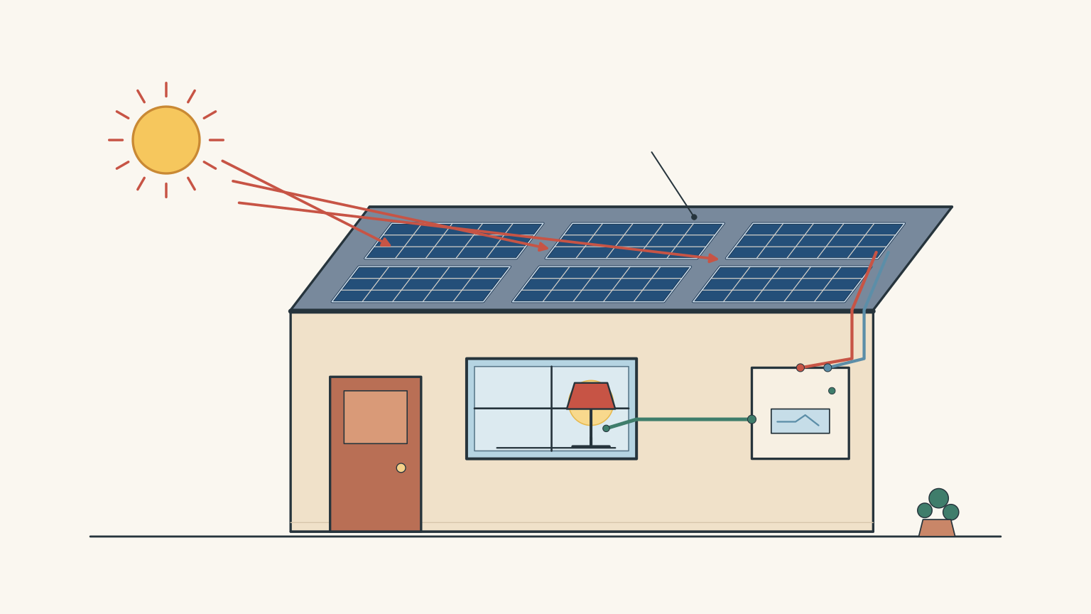
01What happens when a photon enters silicon?
Start with the electron.
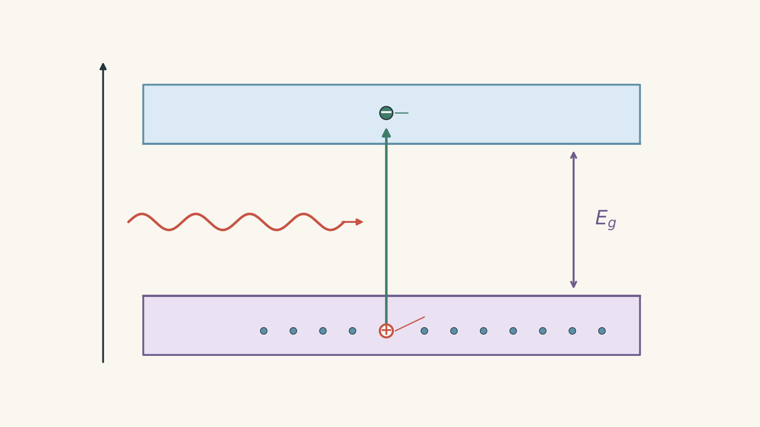
In a piece of silicon, electrons occupy particular ranges of allowed energy called energy bands. Two bands are especially important:
- The valence band contains electrons involved in the bonds holding the silicon structure together.
- The conduction band contains electrons with enough energy to move through the semiconductor and contribute to electrical conduction.
Between these bands is an energy gap called the band gap, \(E_g\).
Think of the valence band and conduction band as two floors in a building. An electron starts on the lower floor. To reach the upper floor, it must receive enough energy to cross the gap between them.
The analogy is useful, but the bands aren’t actual floors or physical locations. They represent allowed electron energies within the semiconductor.
The photon must have enough energy
A photon is a packet of electromagnetic radiation. Its energy depends on the frequency of the light.
\[ E_\gamma = hf \]
Where:
- \(E_\gamma\) is the photon energy, measured in joules (J).
- \(h\) is Planck’s constant, \(6.63\times10^{-34}\text{ J s}\).
- \(f\) is the frequency of the light, measured in hertz (Hz).
Since frequency and wavelength are related by \(c=f\lambda\), we can also write:
\[ E_\gamma = \frac{hc}{\lambda} \]
Here, \(c\) is the speed of light in a vacuum, approximately \(3.00\times10^8\text{ m s}^{-1}\), and \(\lambda\) is the wavelength in metres.
Notice the relationship:
- Higher frequency means greater photon energy.
- Shorter wavelength means greater photon energy.
- Lower frequency means less photon energy.
- Longer wavelength means less photon energy.
For an electron to move from the valence band into the conduction band, the absorbed photon must supply at least the band-gap energy.
\[ E_\gamma \geq E_g \]
For silicon at approximately room temperature, the band gap is about \(1.1\text{ eV}\).
An electronvolt (eV) is a unit of energy:
\[ 1\text{ eV}=1.60\times10^{-19}\text{ J} \]
We can use the silicon band gap to estimate the minimum frequency required to generate an electron-hole pair.
First, convert the band gap into joules:
\[ E_g=1.1(1.60\times10^{-19}) \]
\[ E_g=1.76\times10^{-19}\text{ J} \]
Using \(E=hf\):
\[ f_{\min}=\frac{E_g}{h} \]
\[ f_{\min}= \frac{1.76\times10^{-19}} {6.63\times10^{-34}} \]
\[ f_{\min}\approx2.65\times10^{14}\text{ Hz} \]
This corresponds to a wavelength of approximately:
\[ \lambda_{\max}=\frac{c}{f_{\min}} \]
\[ \lambda_{\max}\approx1.13\times10^{-6}\text{ m} \]
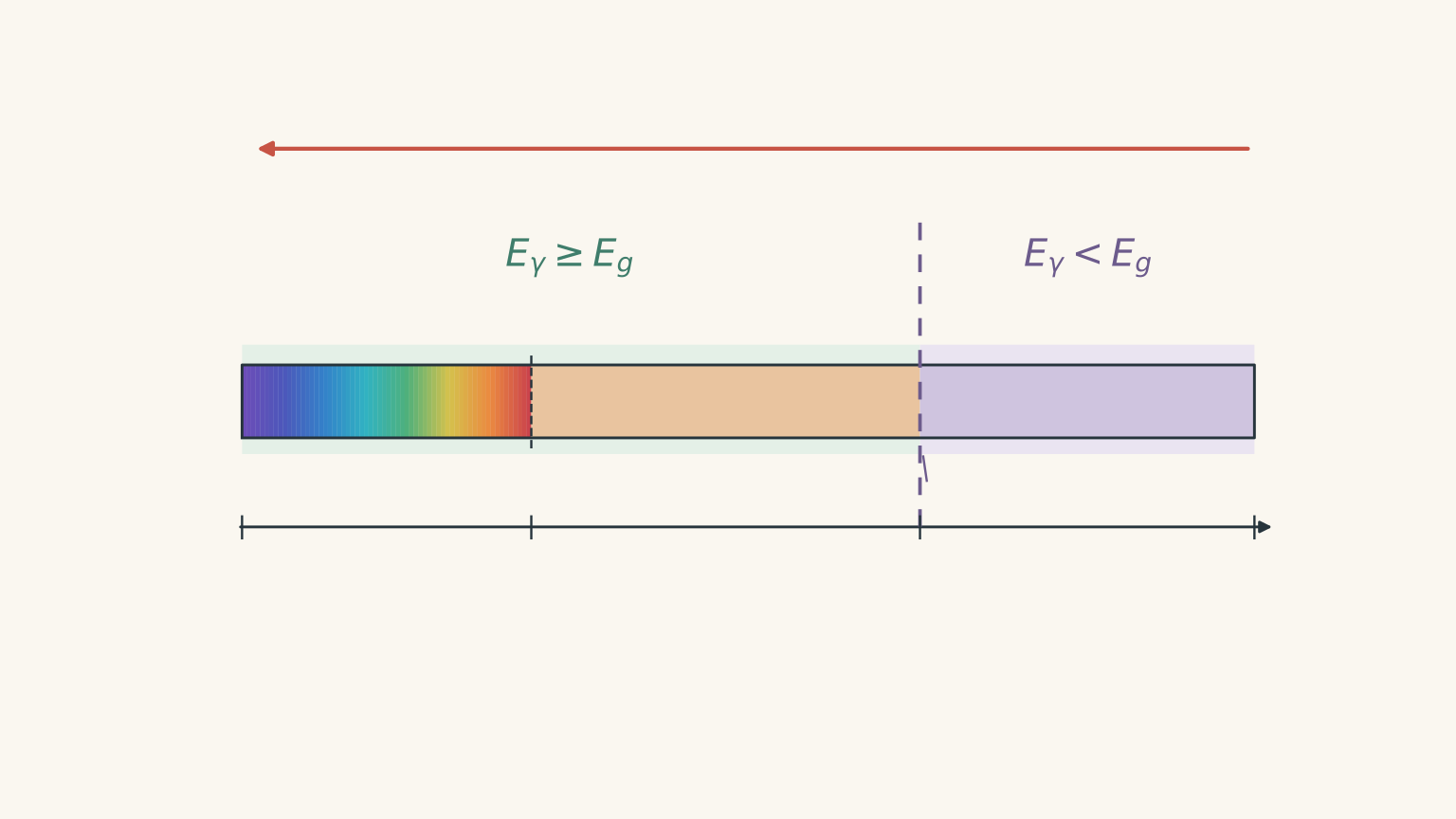
So, in the simplified band-gap model, silicon requires photons with wavelengths shorter than approximately \(1.13\ \mu\text{m}\) to generate electron-hole pairs.
What if the photon has more energy than necessary?
Suppose a photon supplies \(2.5\text{ eV}\), while silicon only requires \(1.1\text{ eV}\).
The electron only needs \(1.1\text{ eV}\) to cross the band gap. What happens to the remaining \(1.4\text{ eV}\)?
In an ordinary silicon solar cell, most of this excess energy is transferred to the semiconductor lattice as thermal energy. The excited electron loses energy as it relaxes towards the bottom of the conduction band.
This is an important limitation.
A photon with twice the band-gap energy does not normally produce twice as many electron-hole pairs in the standard HSC model. One absorbed photon generally produces one pair. The excess energy is mostly converted into heat.
There are therefore two important cases:
| Photon energy | What happens in silicon? |
|---|---|
| \(E_\gamma < E_g\) | The photon cannot generate an electron-hole pair through a normal band-to-band transition. It may pass through or be reflected. |
| \(E_\gamma \geq E_g\) | The photon can generate an electron-hole pair if it is absorbed. Excess energy is mostly converted into heat. |
Make a prediction: If you shine much brighter light on silicon, but every photon has less energy than the band gap, will you eventually generate useful electron-hole pairs?
No, not through the ordinary one-photon process. Increasing intensity increases the number of photons arriving each second. It doesn’t increase the energy of each photon.
This is the first important distinction between light intensity and photon frequency.
02How does a solar cell turn electron-hole pairs into current?
Creating an electron-hole pair is only the beginning.
Imagine that a photon promotes an electron into the conduction band. The electron and the hole are now free to move through the semiconductor.
But there’s a problem: they can recombine.
Recombination occurs when a conduction-band electron falls back into an available state in the valence band, effectively filling the hole. If this happens before the charges are collected, the energy cannot be delivered to the external circuit as useful electrical work.
A solar cell needs a way to separate the two charges before they recombine.
This is where the p-n junction becomes important.
The p-n junction
A typical silicon solar cell contains two differently treated regions of semiconductor:
- The p-type region has holes as its majority mobile charge carriers.
- The n-type region has electrons as its majority mobile charge carriers.
These regions are brought together to form a p-n junction.
When they meet, electrons initially diffuse from the n-type region towards the p-type region. Holes diffuse in the opposite direction.
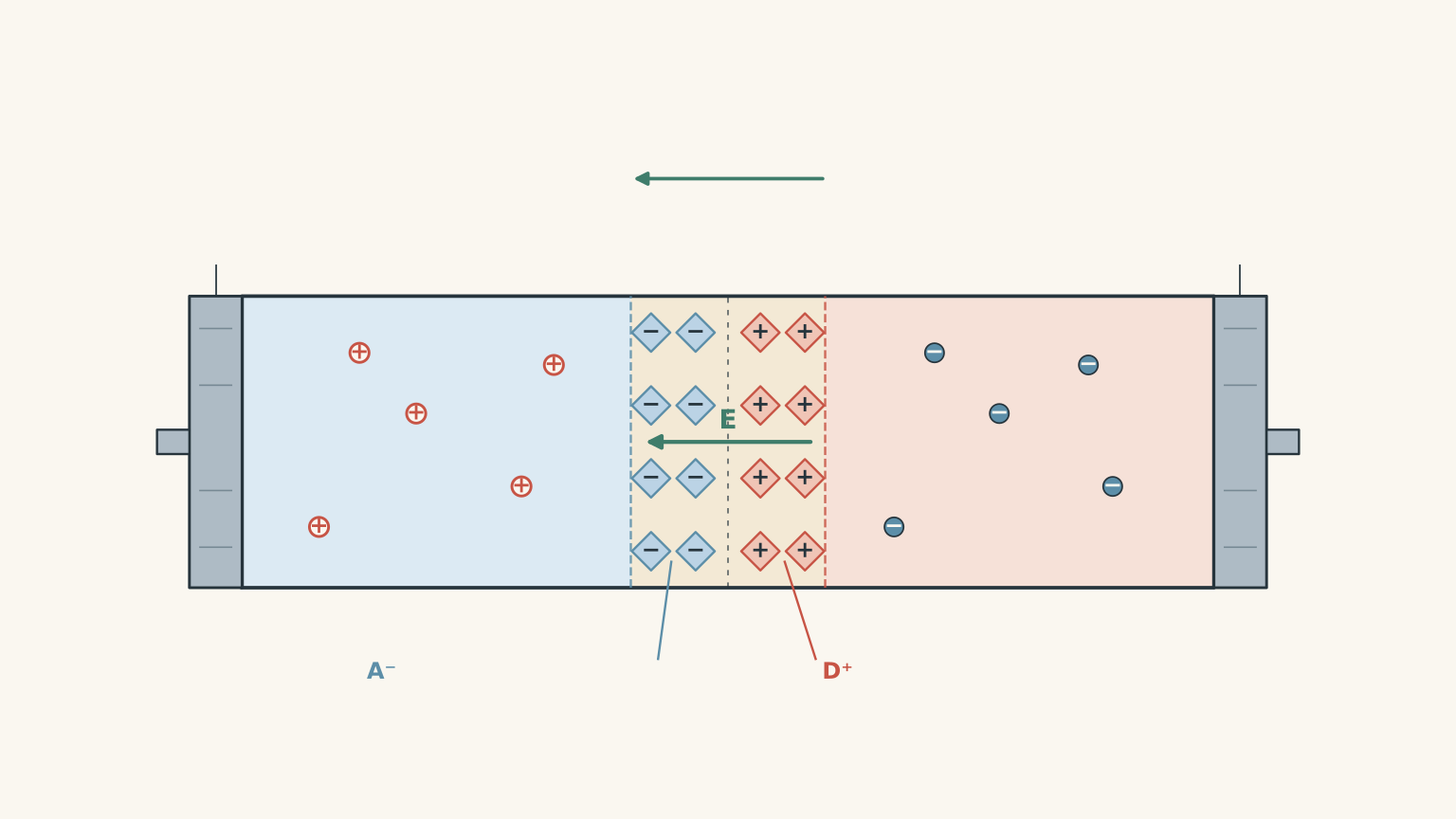
Near the junction, electrons and holes recombine. This leaves behind fixed, electrically charged atoms:
- Positive donor ions on the n-type side.
- Negative acceptor ions on the p-type side.
The region around the junction becomes depleted of mobile charge carriers. It is called the depletion region.
The fixed ions create an internal electric field across this region. Its direction is from the n-type side towards the p-type side.
The internal electric field separates the charges
Now imagine a photon being absorbed in or near the depletion region.
It creates an electron-hole pair:
- The electron has a negative charge.
- The hole behaves as a positive charge carrier.
The internal electric field exerts forces on both.
Remember that negatively charged particles experience a force opposite to the electric field, while positively charged particles experience a force in the same direction.
Therefore:
- The electron moves towards the n-type region.
- The hole moves towards the p-type region.
The electric field has separated the two charges before they can immediately recombine.
Some electron-hole pairs are generated outside the depletion region. These carriers can also contribute if they diffuse towards the junction before recombining. Others are lost through recombination.
This is the internal photovoltaic effect: light generates charge carriers inside a semiconductor, and the junction’s internal electric field helps separate them.
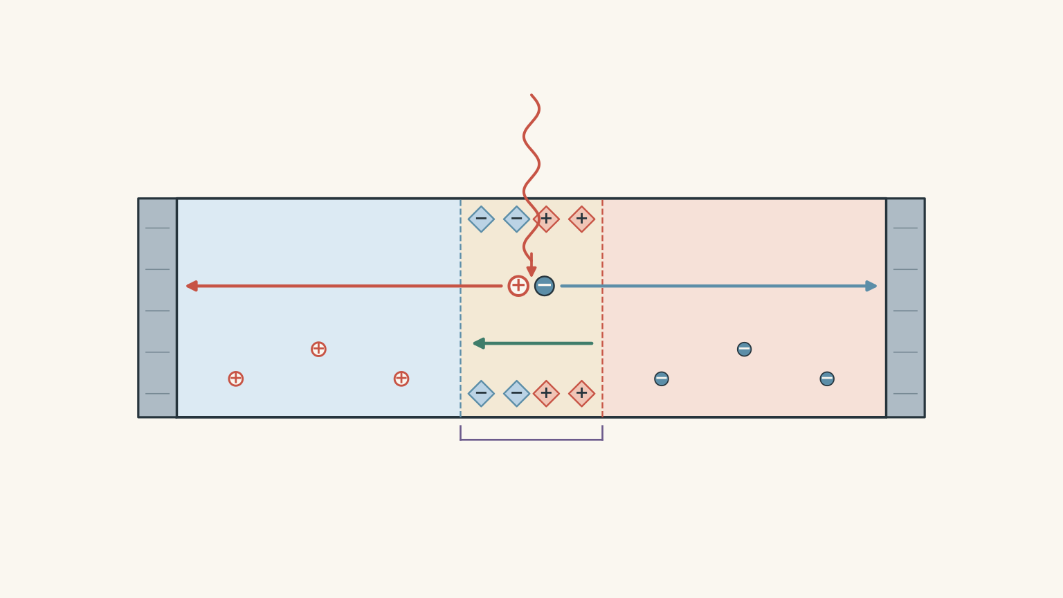
Notice something important: the electric field doesn’t create the electron-hole pair.
The photon supplies the energy needed to create the pair. The electric field separates the charges and helps prevent immediate recombination.
Without the incoming light, the internal field still exists, but it doesn’t provide a continuous supply of energy to an external circuit.
How does this produce an electrical current?
Once the electrons and holes reach their respective regions, they can be collected by the metal contacts.
The separated charges establish a potential difference across the solar cell. The p-type contact becomes positive relative to the n-type contact.
Now consider two situations.
Situation 1: The circuit is open.
The cell is illuminated, but nothing is connected across its terminals.
Electrons and holes continue to be generated and separated. However, there is no complete external path for a sustained current.
Separated charges build up, producing a terminal voltage. As the voltage develops, it opposes further net charge separation. At steady state, recombination balances photogeneration, and the external current is zero.
The cell has a voltage even though it isn’t delivering current.
Situation 2: A load is connected.
Connect a resistor or another electrical device across the terminals.
Electrons can now travel from the n-type contact, through the external circuit, towards the p-type contact. They can then recombine with holes in the cell.
This allows a continuous current to flow while the cell is illuminated.
The direction of conventional current is opposite to the direction of electron flow.
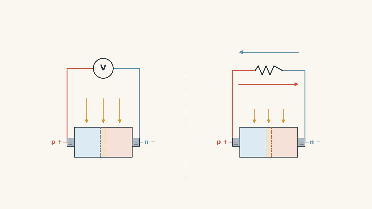
The energy transfer can now be followed:
- A photon is absorbed by the semiconductor.
- An electron gains enough energy to enter the conduction band.
- An electron-hole pair is created.
- The internal electric field separates the charges.
- The contacts collect the carriers.
- Charge flows through the external circuit, transferring electrical energy to the load.
The light supplies the energy. The junction field controls the separation of charge. The external circuit provides a path through which electrical energy can be transferred.
03Solar cells versus phototubes: two different effects
A solar cell and a phototube both use light to produce an electrical response.
However, the mechanisms are fundamentally different.
A phototube uses the photoelectric effect. A solar cell uses the internal photovoltaic effect.
How a phototube works
A phototube contains two electrodes inside an evacuated glass tube:
- A photosensitive metal cathode.
- A positively charged anode.
When light strikes the cathode, photons can transfer energy to electrons in the metal.
If an electron receives enough energy to escape the metal surface, it is emitted into the vacuum. This is called photoelectric emission.
The electron can then travel through the vacuum towards the positively charged anode, producing a photocurrent in the external circuit.
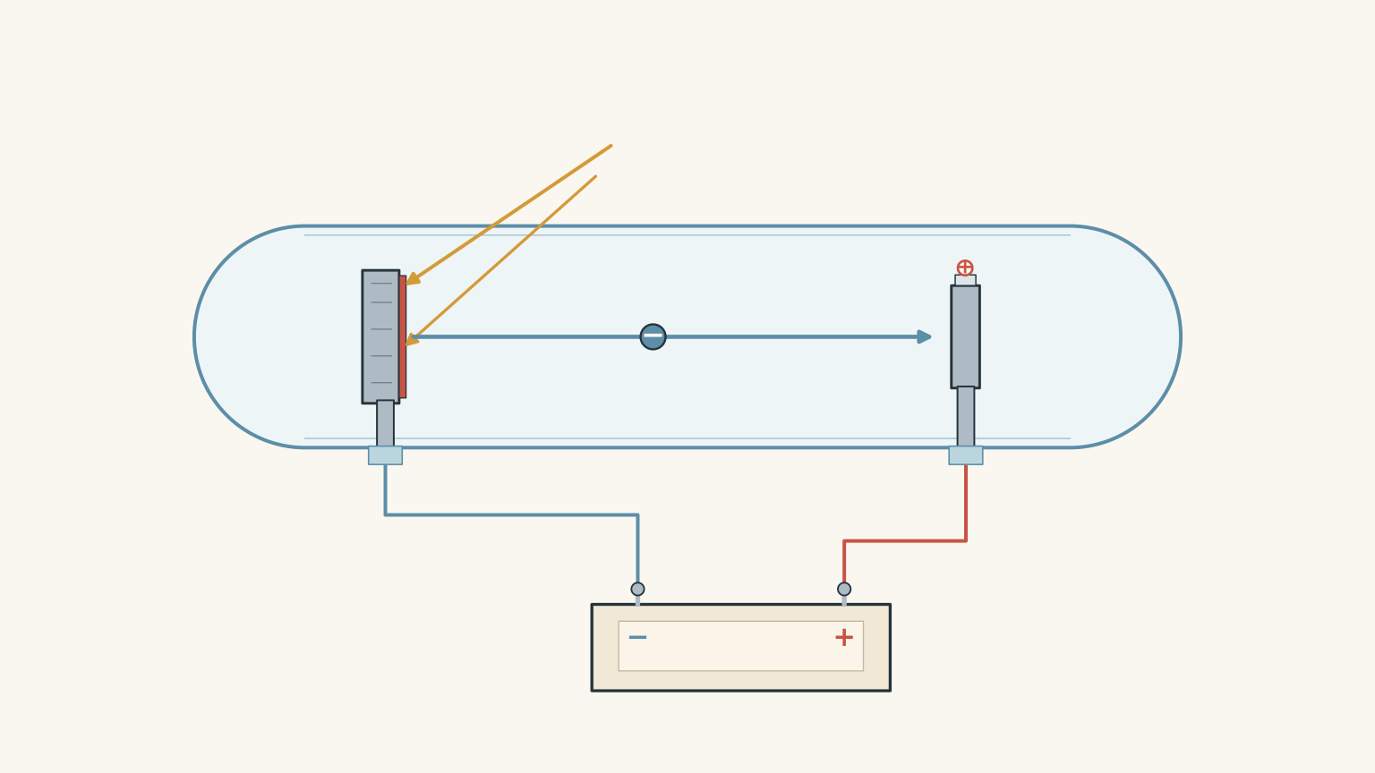
The key requirement is that the photon must supply enough energy to overcome the metal’s work function, \(\phi\).
The work function is the minimum energy required to remove an electron from the metal surface.
Therefore, the threshold condition is:
\[ hf\geq\phi \]
The minimum frequency is:
\[ f_0=\frac{\phi}{h} \]
If the photon energy is below the work function, no electron is emitted in the ordinary one-photon photoelectric effect.
Increasing the brightness doesn’t solve this problem. You can send more photons towards the cathode, but each photon still has insufficient energy.
For photons above the threshold, the maximum kinetic energy of an emitted electron is:
\[ E_{k,\max}=hf-\phi \]
Increasing the frequency increases the maximum kinetic energy of the emitted electrons.
Increasing the intensity, provided the frequency is above threshold, increases the number of photons arriving per second and therefore generally increases the number of emitted electrons.
Put the two devices side by side
| Feature | Solar cell | Phototube |
|---|---|---|
| Starting material | Semiconductor | Photosensitive metal |
| Minimum photon energy | Band-gap energy, \(E_g\) | Work function, \(\phi\) |
| What happens to the electron? | Moves into the conduction band but remains inside the semiconductor | Escapes the metal surface into a vacuum |
| Positive charge left behind | A hole in the valence band | An electron deficiency in the metal |
| Role of electric field | Internal p-n junction field separates electrons and holes | Applied electric field attracts emitted electrons towards the anode |
| Main process | Internal photovoltaic effect | Photoelectric emission |
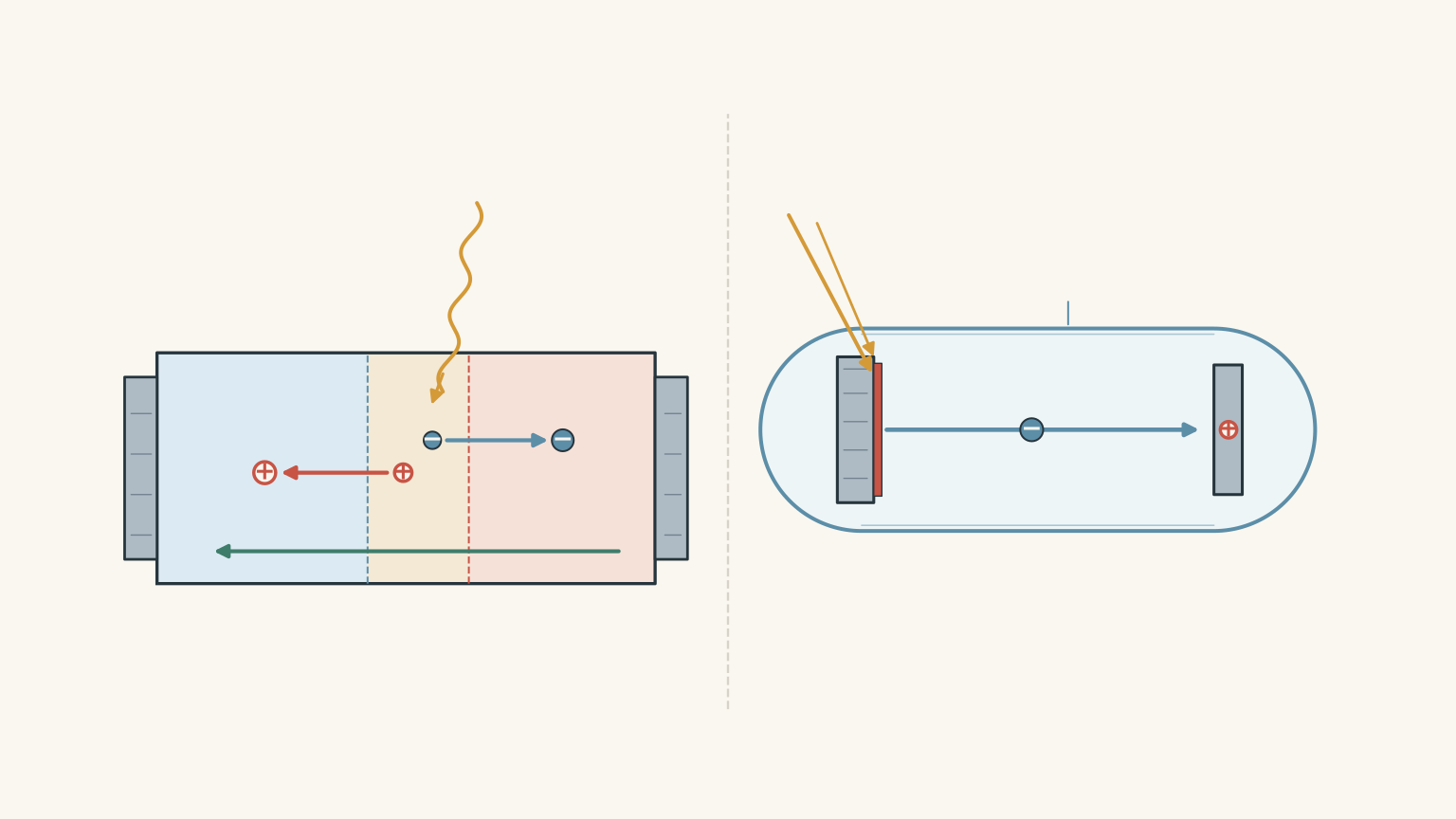
The biggest distinction is the destination of the electron.
In a phototube, the electron must escape the metal.
In a solar cell, the electron only needs enough energy to enter the conduction band. It remains inside the semiconductor and is separated from the hole by the internal electric field.
This is why you should never automatically apply the metal work-function threshold to a semiconductor solar cell. They have different energy requirements.
04Worked examples
Worked example: Can green light generate electron-hole pairs?
A silicon solar cell is illuminated with green light of wavelength \(520\text{ nm}\). Calculate the energy of one photon in electronvolts and determine whether it can generate an electron-hole pair.
Take the band gap of silicon to be \(1.1\text{ eV}\).
Step 1
\[ \lambda=520\times10^{-9}\text{ m} \]
\[ \lambda=5.20\times10^{-7}\text{ m} \]
Step 2
Using:
\[ f=\frac{c}{\lambda} \]
Substitute:
\[ f=\frac{3.00\times10^8} {5.20\times10^{-7}} \]
\[ f=5.77\times10^{14}\text{ Hz} \]
Step 3
\[ E_\gamma=hf \]
\[ E_\gamma= (6.63\times10^{-34}) (5.77\times10^{14}) \]
\[ E_\gamma=3.83\times10^{-19}\text{ J} \]
Convert into electronvolts:
\[ E_\gamma= \frac{3.83\times10^{-19}} {1.60\times10^{-19}} \]
\[ E_\gamma=2.39\text{ eV} \]
Step 4
\[ 2.39\text{ eV}>1.1\text{ eV} \]
Therefore, the photon has sufficient energy to generate an electron-hole pair if it is absorbed by the silicon.
The excess energy is:
\[ E_{\text{excess}}=2.39-1.1 \]
\[ E_{\text{excess}}=1.29\text{ eV} \]
Most of this excess energy is eventually transferred to the semiconductor as heat.
The important result is that the photon creates a charge pair, not an electron with \(2.39\text{ eV}\) of useful electrical energy available to the external circuit.
Worked example: Calculate the electrical output of a solar panel
A solar panel has an area of \(1.6\text{ m}^2\). It receives sunlight with an irradiance of \(750\text{ W m}^{-2}\).
The panel converts 20% of the incoming solar power into electrical power. If its operating voltage is \(24\text{ V}\), calculate the electrical current delivered by the panel.
Step 1
Irradiance is power received per unit area.
Therefore:
\[ P_{\text{in}}=GA \]
Where:
- \(G\) is the solar irradiance in \(\text{W m}^{-2}\).
- \(A\) is the panel area in \(\text{m}^2\).
Substitute:
\[ P_{\text{in}}=750\times1.6 \]
\[ P_{\text{in}}=1200\text{ W} \]
The panel receives \(1200\text{ W}\) of solar power.
Step 2
Efficiency is the fraction of incoming power converted into useful electrical power.
\[ \eta=\frac{P_{\text{out}}}{P_{\text{in}}} \]
Rearrange:
\[ P_{\text{out}}=\eta P_{\text{in}} \]
Substitute:
\[ P_{\text{out}}=0.20\times1200 \]
\[ P_{\text{out}}=240\text{ W} \]
The panel delivers \(240\text{ W}\) of electrical power.
Step 3
Electrical power is related to voltage and current by:
\[ P=VI \]
Rearrange:
\[ I=\frac{P}{V} \]
Substitute:
\[ I=\frac{240}{24} \]
\[ I=10\text{ A} \]
The final answer is:
\[ \boxed{I=10\text{ A}} \]
The panel delivers \(10\text{ A}\) at \(24\text{ V}\), giving an electrical output of \(240\text{ W}\).
Notice that the incoming solar power was \(1200\text{ W}\), but only \(240\text{ W}\) became electrical output. The remaining energy is not all lost through one mechanism. Reflection, transmission, thermalisation, recombination, and electrical resistance all contribute to the difference.
05What limits a solar cell’s output?
A solar cell cannot convert every incoming photon into useful electrical energy.
Several processes limit its efficiency.
| Limitation | What happens? |
|---|---|
| Reflection | Some incoming photons never enter the semiconductor. |
| Below-band-gap photons | Their energy is insufficient to generate normal electron-hole pairs. |
| Excess photon energy | Energy above the band gap is mostly converted into heat. |
| Recombination | Some electrons recombine with holes before being collected. |
| Electrical resistance | Some electrical energy is dissipated as heat in the cell and its connections. |
There is also a common misconception about voltage.
A photon with an energy of \(2.4\text{ eV}\) does not mean that a solar cell automatically produces \(2.4\text{ V}\).
Voltage measures electrical energy transferred per unit charge:
\[ V=\frac{W}{q} \]
Here, \(W\) is the energy transferred and \(q\) is the charge.
The photon energy is the energy supplied to an individual absorption event. The terminal voltage is determined by the behaviour of the illuminated semiconductor junction, the separation and recombination of carriers, and the operating conditions.
In a real silicon solar cell, the output voltage is considerably lower than the band-gap energy expressed in volts.
Keep these three ideas separate:
- Photon energy determines whether an electron can cross the band gap.
- The internal electric field helps separate the electron and hole.
- The external circuit determines how electrical energy is delivered to a load.
That separation of ideas will help you avoid many common mistakes in questions about photovoltaic cells.
06Questions and solutions
Question 1
A silicon solar cell is illuminated with monochromatic light of wavelength \(480\text{ nm}\).
Calculate the energy of one photon in electronvolts. Determine whether an absorbed photon can generate an electron-hole pair in silicon.
Use:
- \(h=6.63\times10^{-34}\text{ J s}\)
- \(c=3.00\times10^8\text{ m s}^{-1}\)
- \(1\text{ eV}=1.60\times10^{-19}\text{ J}\)
- \(E_g=1.1\text{ eV}\)
Solution 1
Yes. Each photon has approximately \(2.59\text{ eV}\) of energy, which is greater than silicon’s band gap of \(1.1\text{ eV}\).
Step 1: Convert the wavelength into metres.
\[ \lambda=480\times10^{-9}\text{ m} \]
\[ \lambda=4.80\times10^{-7}\text{ m} \]
Step 2: Calculate the photon frequency.
\[ f=\frac{c}{\lambda} \]
\[ f=\frac{3.00\times10^8} {4.80\times10^{-7}} \]
\[ f=6.25\times10^{14}\text{ Hz} \]
Step 3: Calculate the photon energy.
\[ E_\gamma=hf \]
\[ E_\gamma= (6.63\times10^{-34}) (6.25\times10^{14}) \]
\[ E_\gamma=4.14\times10^{-19}\text{ J} \]
Convert into electronvolts:
\[ E_\gamma= \frac{4.14\times10^{-19}} {1.60\times10^{-19}} \]
\[ E_\gamma=2.59\text{ eV} \]
Step 4: Compare the photon energy with the band gap.
\[ 2.59\text{ eV}>1.1\text{ eV} \]
The photon has sufficient energy to promote an electron into the conduction band.
It can therefore generate an electron-hole pair if absorbed.
The excess energy is:
\[ E_{\text{excess}}=2.59-1.1 \]
\[ E_{\text{excess}}=1.49\text{ eV} \]
Most of this excess energy is dissipated as heat.
The important distinction is that the photon supplies enough energy to create the pair, but its entire energy does not become useful electrical output.
Question 2
A silicon solar cell has a band-gap energy of \(1.1\text{ eV}\).
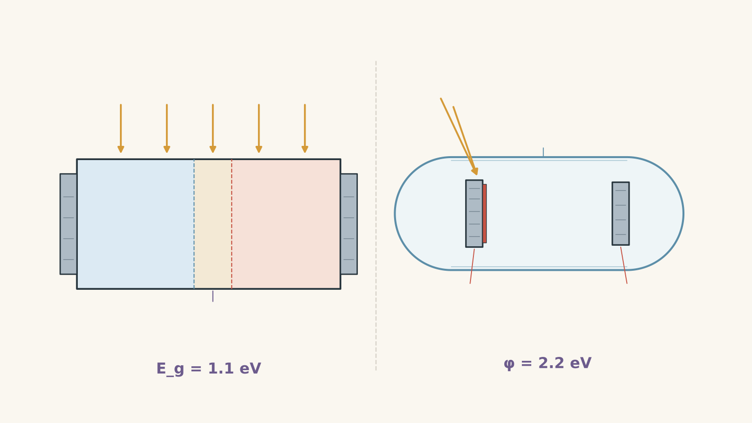
A phototube has a metal cathode with a work function of \(2.2\text{ eV}\).
Both devices are illuminated by monochromatic light with a photon energy of \(1.6\text{ eV}\).
Assume each photon reaching the silicon is absorbed.
(a) Determine whether each device can produce a photoresponse.
(b) A student suggests increasing the light intensity by a factor of 100 to make the phototube emit electrons. Explain whether this will work.
Solution 2
The silicon solar cell can generate electron-hole pairs, but the phototube cannot emit electrons under this illumination.
Part (a): Compare the two energy thresholds.
For the silicon solar cell:
\[ E_\gamma=1.6\text{ eV} \]
\[ E_g=1.1\text{ eV} \]
Since:
\[ 1.6>1.1 \]
The photon has enough energy to promote an electron from the valence band into the conduction band.
An electron-hole pair can therefore be generated inside the silicon.
For the phototube:
\[ E_\gamma=1.6\text{ eV} \]
\[ \phi=2.2\text{ eV} \]
Since:
\[ 1.6<2.2 \]
The photon does not have enough energy to overcome the metal’s work function.
No electron can escape the cathode through the ordinary photoelectric effect.
Part (b): Consider increasing the intensity.
Increasing the intensity increases the number of photons arriving each second.
However, it does not increase the energy of an individual photon.
Every photon still has an energy of \(1.6\text{ eV}\), which is below the work function of \(2.2\text{ eV}\).
Therefore, increasing the intensity by a factor of 100 will not produce photoelectric emission in the ordinary one-photon model.
This question tests an important distinction: the threshold depends on the energy of each photon, not the total energy arriving at the surface.
Question 3
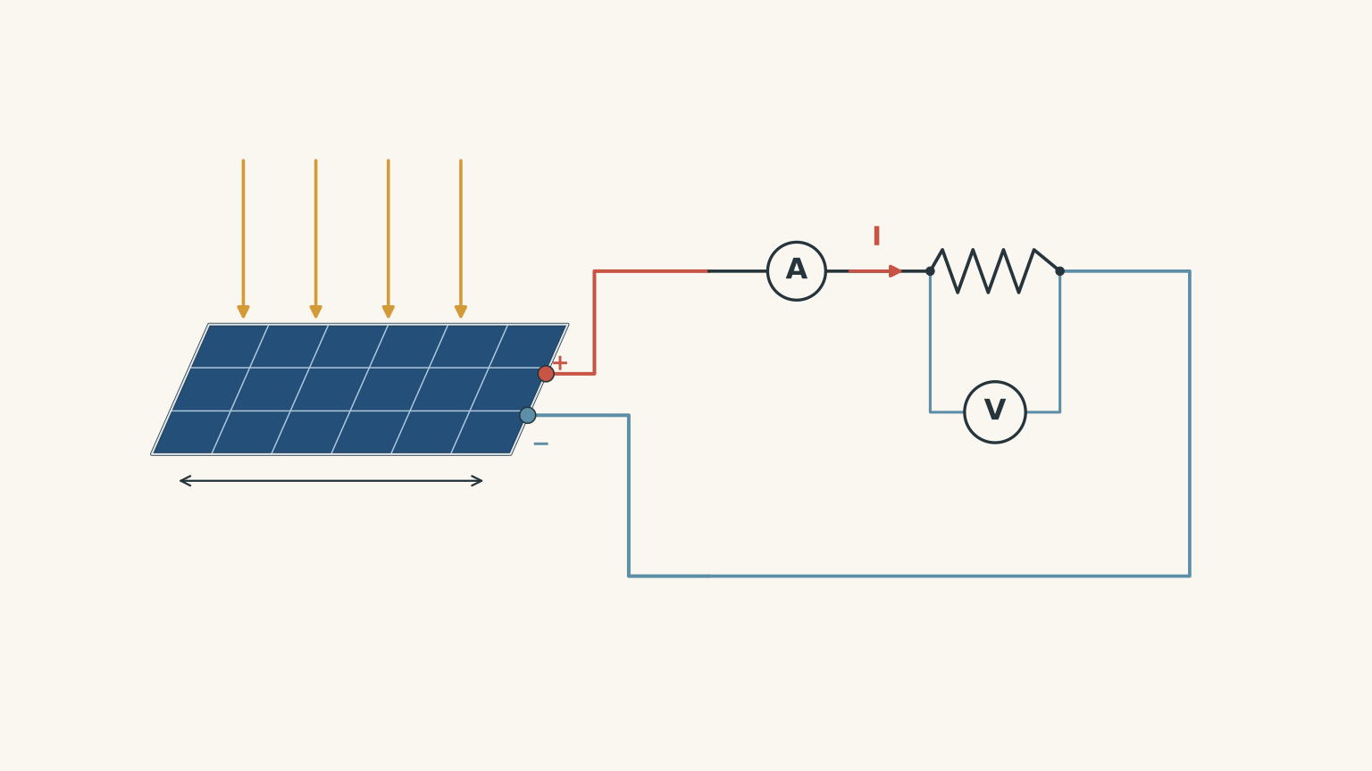
A solar array has a total surface area of \(2.4\text{ m}^2\). It receives sunlight with an irradiance of \(680\text{ W m}^{-2}\).
The array has an efficiency of 16% and operates at a terminal voltage of \(32\text{ V}\).
Calculate:
(a) The incoming solar power.
(b) The electrical output power.
(c) The current delivered by the array.
Assume the stated efficiency applies at the operating point.
Solution 3
The array receives \(1632\text{ W}\) of solar power, converts approximately \(261\text{ W}\) into electrical power, and delivers a current of approximately \(8.16\text{ A}\).
Part (a): Calculate the incoming solar power.
Use:
\[ P_{\text{in}}=GA \]
Substitute:
\[ P_{\text{in}}=680\times2.4 \]
\[ \boxed{P_{\text{in}}=1632\text{ W}} \]
The array receives \(1632\text{ W}\) of incoming solar energy per second.
Part (b): Calculate the electrical output power.
Efficiency is:
\[ \eta=\frac{P_{\text{out}}}{P_{\text{in}}} \]
Rearrange:
\[ P_{\text{out}}=\eta P_{\text{in}} \]
Substitute:
\[ P_{\text{out}}=0.16\times1632 \]
\[ \boxed{P_{\text{out}}=261.12\text{ W}} \]
The array converts approximately \(261\text{ W}\) into electrical power.
Part (c): Calculate the output current.
Use:
\[ P=VI \]
Rearrange:
\[ I=\frac{P}{V} \]
Substitute:
\[ I=\frac{261.12}{32} \]
\[ \boxed{I=8.16\text{ A}} \]
The array delivers approximately \(8.16\text{ A}\) at \(32\text{ V}\).
A useful check is to compare the electrical output with the incoming power. The output is 16% of the input, as required by the stated efficiency.
Question 4
A solar cell is illuminated continuously.
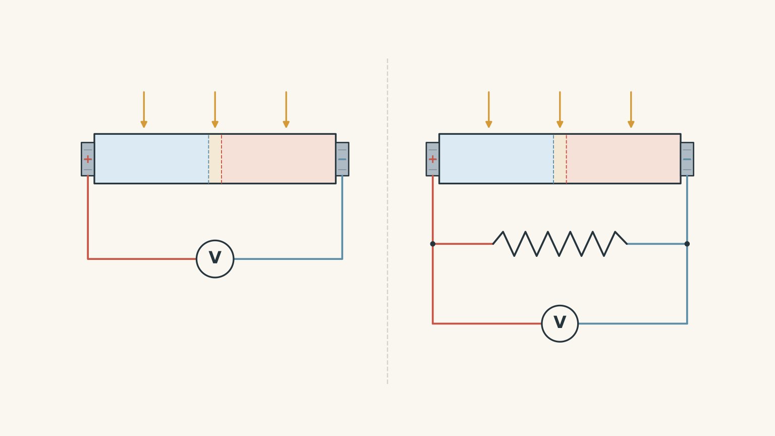
Initially, its terminals are connected only to a high-resistance voltmeter. The voltmeter measures a potential difference of \(0.58\text{ V}\).
A resistor is then connected across the solar cell. The terminal voltage settles at \(0.46\text{ V}\), and a current flows through the resistor.
A student argues:
“The solar cell must stop generating electron-hole pairs when the circuit is open. Otherwise, there would be a current.”
Explain why this statement is incorrect.
In your answer, discuss:
- Electron-hole pair generation.
- The role of the internal electric field.
- The difference between open-circuit and loaded operation.
- The direction of electron flow and conventional current.
Solution 4
The student is incorrect because electron-hole pairs continue to be generated under illumination even when the external circuit is open. The difference is whether the separated charges have a complete external path through which to flow.
Open-circuit operation
Photons continue to be absorbed by the semiconductor.
When a photon has sufficient energy, it can promote an electron into the conduction band, leaving a hole behind.
The internal electric field separates these charges:
- Electrons move towards the n-type region.
- Holes move towards the p-type region.
However, the external circuit is open, so there is no complete path for sustained current.
The separated charges establish a potential difference across the terminals. This is called the open-circuit voltage.
At steady state, photogeneration is balanced by recombination, so the net external current is zero.
The measured \(0.58\text{ V}\) is therefore entirely consistent with an illuminated solar cell that is not delivering current to a load.
Loaded operation
When the resistor is connected, the external circuit is complete.
Electrons can move from the n-type contact through the resistor towards the p-type contact.
Conventional current flows in the opposite direction, from the p-type contact towards the n-type contact.
The separated charges can now be continuously transferred through the external circuit, delivering electrical energy to the resistor.
Why does the voltage decrease?
The terminal voltage falls from \(0.58\text{ V}\) to \(0.46\text{ V}\) because the cell is now supplying current.
The cell has a particular current-voltage relationship. Internal resistance and the behaviour of the illuminated junction contribute to the difference between its open-circuit voltage and its operating voltage under load.
The key distinction is:
- Open circuit: voltage exists, but no sustained external current flows.
- Connected load: voltage and current are both present, allowing electrical power to be delivered.
The generation of electron-hole pairs does not depend on whether an external load is connected. The load determines how the separated charges can transfer energy through the circuit.
Question 5
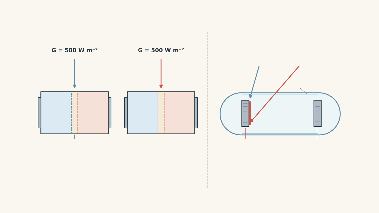
Two identical silicon solar cells are illuminated by different monochromatic light sources.
Both sources have the same irradiance of \(500\text{ W m}^{-2}\).
- Cell A receives light with a wavelength of \(450\text{ nm}\).
- Cell B receives light with a wavelength of \(650\text{ nm}\).
Both cells have a band-gap energy of \(1.1\text{ eV}\).
Assume:
- Both cells have the same surface area and temperature.
- Both wavelengths have the same fraction of their incoming energy absorbed by the silicon.
- Every absorbed photon generates exactly one electron-hole pair.
- Every generated pair is collected.
- Neither cell is operating in a saturated regime.
A separate phototube has a metal cathode with a work function of \(2.0\text{ eV}\). It is exposed to each light source in turn.
(a) Calculate the energy of a photon from each light source in electronvolts.
(b) Determine whether each light source can generate electron-hole pairs in silicon.
(c) Calculate the ratio of the short-circuit currents produced by the two solar cells.
(d) Determine which light source can produce photoelectric emission from the phototube.
(e) A student claims:
“The 450 nm light must produce a greater solar-cell current because each of its photons has more energy.”
Evaluate this claim, explaining the difference between photon energy and photon flux.
Solution 5
Cell B, illuminated by the \(650\text{ nm}\) light, produces \(1.44\) times the short-circuit current of Cell A under the stated assumptions. Both wavelengths can generate electron-hole pairs in silicon, but only the \(450\text{ nm}\) light can eject electrons from the phototube.
This result is initially surprising because the \(450\text{ nm}\) photons carry more energy individually.
The important detail is that both light sources have the same irradiance. They deliver the same energy per second per unit area, not the same number of photons.
Part (a): Calculate the photon energies.
For Cell A:
\[ \lambda_A=450\times10^{-9}\text{ m} \]
First calculate the frequency:
\[ f_A=\frac{3.00\times10^8} {450\times10^{-9}} \]
\[ f_A=6.67\times10^{14}\text{ Hz} \]
Now calculate the photon energy:
\[ E_A=hf_A \]
\[ E_A=(6.63\times10^{-34}) (6.67\times10^{14}) \]
\[ E_A=4.42\times10^{-19}\text{ J} \]
Convert into electronvolts:
\[ E_A= \frac{4.42\times10^{-19}} {1.60\times10^{-19}} \]
\[ \boxed{E_A=2.76\text{ eV}} \]
For Cell B:
\[ \lambda_B=650\times10^{-9}\text{ m} \]
Calculate the frequency:
\[ f_B=\frac{3.00\times10^8} {650\times10^{-9}} \]
\[ f_B=4.62\times10^{14}\text{ Hz} \]
Calculate the photon energy:
\[ E_B=hf_B \]
\[ E_B=(6.63\times10^{-34}) (4.62\times10^{14}) \]
\[ E_B=3.06\times10^{-19}\text{ J} \]
Convert into electronvolts:
\[ E_B= \frac{3.06\times10^{-19}} {1.60\times10^{-19}} \]
\[ \boxed{E_B=1.91\text{ eV}} \]
As expected, the shorter wavelength produces the more energetic photon.
Part (b): Determine whether each wavelength can generate electron-hole pairs.
The silicon band gap is:
\[ E_g=1.1\text{ eV} \]
For Cell A:
\[ 2.76>1.1 \]
Therefore, the \(450\text{ nm}\) photons have enough energy to generate electron-hole pairs.
For Cell B:
\[ 1.91>1.1 \]
Therefore, the \(650\text{ nm}\) photons can also generate electron-hole pairs.
Both wavelengths are above the silicon absorption threshold.
Part (c): Compare the short-circuit currents.
This is the crucial part of the question.
Irradiance is energy arriving per second per unit area.
Both cells receive the same irradiance, so they receive the same total energy per second per unit area.
However, each \(450\text{ nm}\) photon carries more energy than each \(650\text{ nm}\) photon.
Consequently, there must be fewer \(450\text{ nm}\) photons arriving each second.
We can calculate the relationship using photon flux.
Photon flux, \(\Phi\), is the number of photons arriving per second per unit area.
For a monochromatic light source:
\[ \Phi=\frac{G}{E_\gamma} \]
Where \(G\) is the irradiance and \(E_\gamma\) is the energy of an individual photon.
Since both sources have the same irradiance:
\[ \frac{\Phi_B}{\Phi_A} = \frac{E_A}{E_B} \]
Substitute:
\[ \frac{\Phi_B}{\Phi_A} = \frac{2.76}{1.91} \]
\[ \frac{\Phi_B}{\Phi_A}\approx1.44 \]
Therefore, Cell B receives approximately 1.44 times as many photons per second per unit area.
Under the assumptions in the question, each absorbed photon produces one collected electron-hole pair.
Each pair contributes one elementary charge to the short-circuit current.
Therefore, the current is proportional to the photon flux:
\[ \frac{I_B}{I_A} = \frac{\Phi_B}{\Phi_A} \]
\[ \boxed{\frac{I_B}{I_A}=1.44} \]
Cell B produces approximately 44% more short-circuit current than Cell A.
Part (d): Determine which light source produces photoelectric emission.
The phototube has a work function of:
\[ \phi=2.0\text{ eV} \]
For the \(450\text{ nm}\) light:
\[ E_A=2.76\text{ eV} \]
Since:
\[ 2.76>2.0 \]
The photon has enough energy to eject an electron from the metal cathode.
The maximum kinetic energy of an emitted electron is:
\[ E_{k,\max}=E_A-\phi \]
\[ E_{k,\max}=2.76-2.0 \]
\[ E_{k,\max}=0.76\text{ eV} \]
Therefore, the \(450\text{ nm}\) light produces photoelectric emission.
For the \(650\text{ nm}\) light:
\[ E_B=1.91\text{ eV} \]
Since:
\[ 1.91<2.0 \]
The photon energy is below the work function.
Therefore, the \(650\text{ nm}\) light cannot produce photoelectric emission in this phototube.
Part (e): Evaluate the student’s claim.
The claim is incorrect.
The student has confused the energy carried by each photon with the number of photons arriving each second.
The \(450\text{ nm}\) photons are individually more energetic, but there are fewer of them because the two light sources have the same irradiance.
The \(650\text{ nm}\) photons have less energy individually, but more photons arrive each second. Since both wavelengths can generate electron-hole pairs in silicon, the larger photon flux produces the larger short-circuit current.
There is another important detail.
The excess energy above the silicon band gap is mostly converted into heat. The extra energy carried by the \(450\text{ nm}\) photons does not automatically become extra electrical current.
This is why photon energy and photon flux must be considered separately.
The two devices also respond differently to the same light. Both wavelengths can generate carriers inside silicon, but only the \(450\text{ nm}\) photons have enough energy to eject electrons from the phototube’s metal cathode.
Once you understand how photons generate charge carriers and how the p-n junction separates them, the next useful concept is the solar cell’s current-voltage (I-V) characteristic.
An I-V graph shows how the current and voltage change as the electrical load changes. It also allows you to identify the maximum-power operating point, where the solar cell delivers the greatest electrical power rather than simply the greatest current or voltage.